
IRIS photovoltaic lab
The IRIS photovoltaic lab in Berlin Adlershof focuses on precision fabrication and optical-electronic characterization of perovskite solar cells.
With strong capabilities in microscopy and thin-film analysis, the lab is suited for advanced studies on optical phenomena, material interfaces, and stability under variable illumination and environmental conditions.
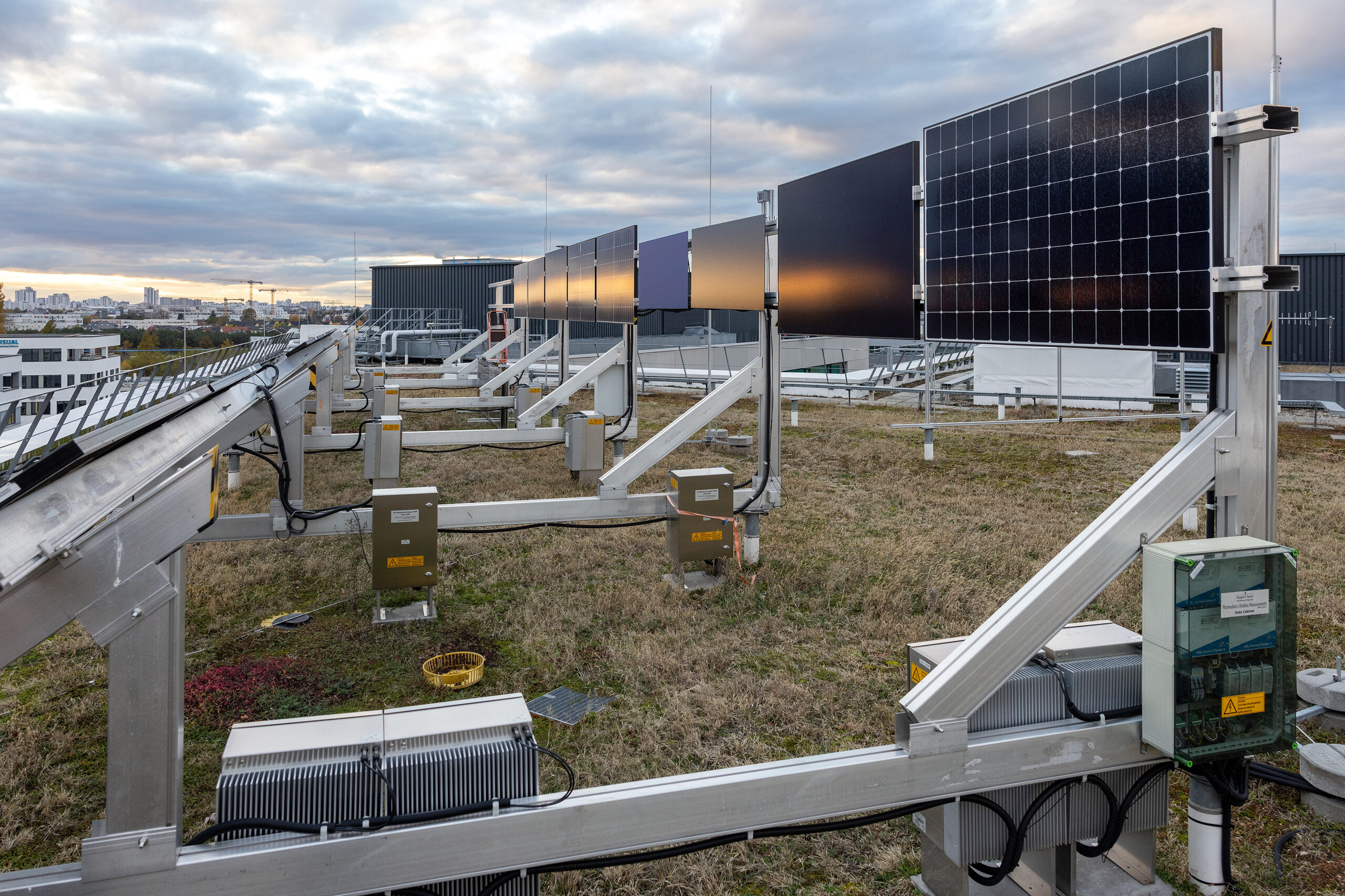

Overview
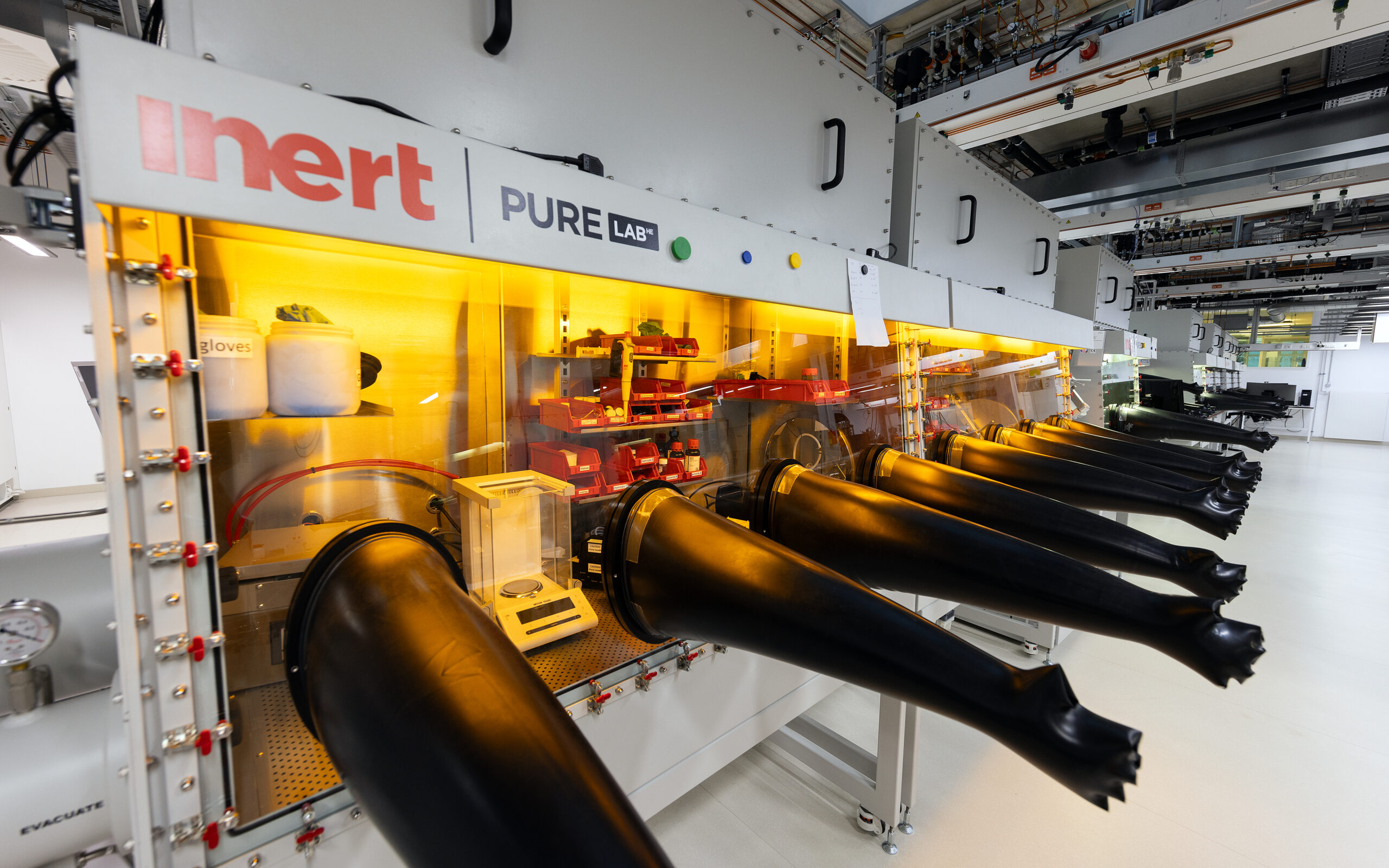
The IRIS photovoltaic lab at Berlin-Adlershof is dedicated to high-precision fabrication and comprehensive optical and electronic characterization of thin-film perovskite solar cells. The facility provides access to state-of-the-art microscopy and surface-sensitive analytical techniques, enabling the lab to investigate complex material interfaces and their functional impact on device performance. With a strong foundation in spectroscopy and thin-film processing, IRIS supports both basic and application-oriented research into advanced photovoltaic systems.
Detailed Description
Purpose: The research focuses on the in-depth optical and morphological analysis of perovskite absorber layers to uncover structure–function relationships that govern device performance. A key emphasis lies in interface engineering, particularly the correlation between structural features and optoelectronic behavior across material boundaries. The lab leverages advanced deposition techniques such as atomic layer deposition (ALD) and thermal evaporation to develop and optimize transport layers with high precision. Through spectroscopy-driven investigations, IRIS contributes to a fundamental understanding of material dynamics—aiming to systematically enhance the efficiency and long-term stability of perovskite-based photovoltaic devices.
Unique Features
- Advanced optical spectroscopy for interface and thin-film analysis
- Surface and structural characterization at nanometer scale
- Focused development of transport layers using ALD and evaporation
- Non-invasive methods for evaluating perovskite degradation and phase stability
Processing Capabilities
Active Layers
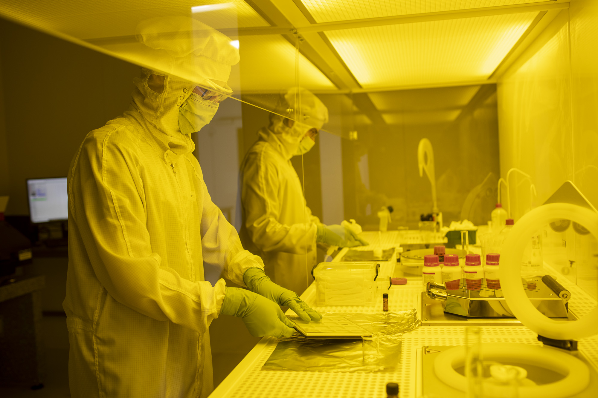
- Spin coating
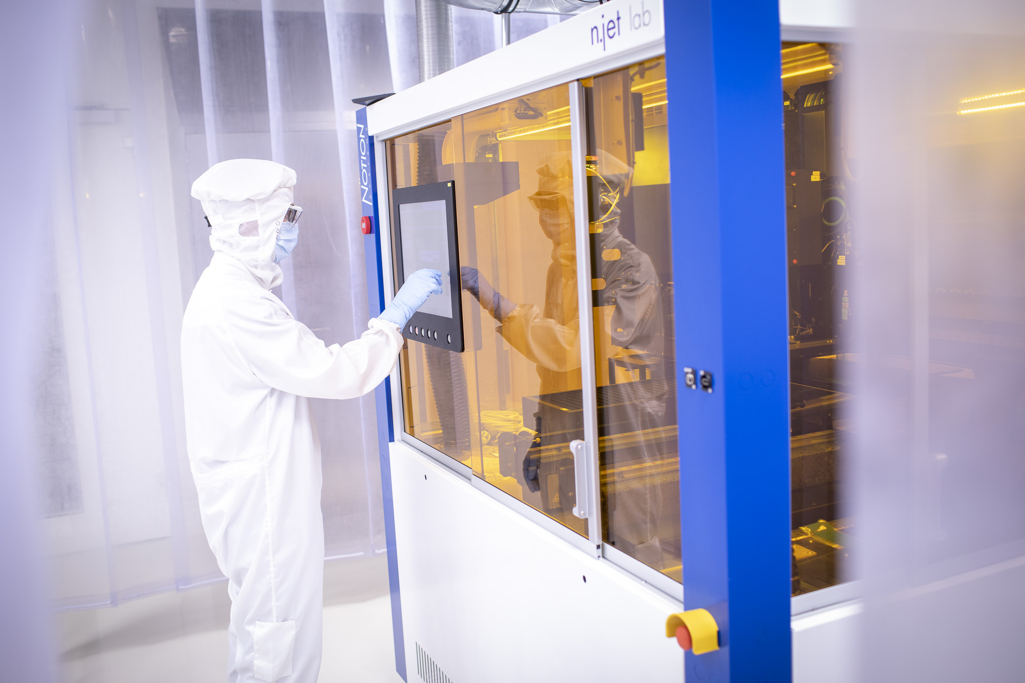
- Inkjet printing
Electrodes
- Thermal evaporation
- Off-line packaging setup
Transport Layers
- Thermal evaporation
- Atomic layer deposition (ALD)
Characterization Capabilities
Devices
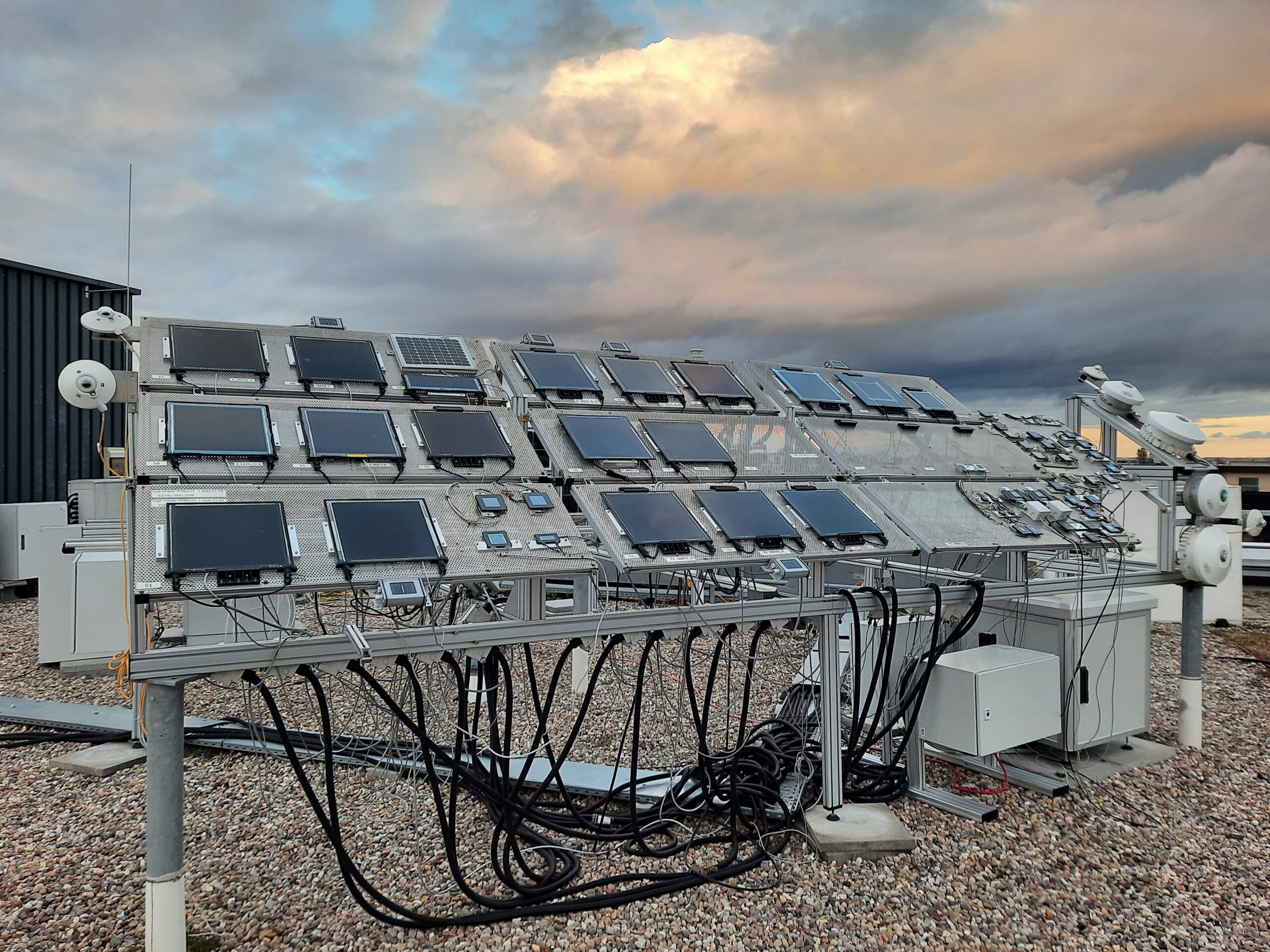
- Solar simulators (Xenon source, indoor testing; LED for outdoor setups)
- External quantum efficiency (EQE) measurement (outdoor)
Stability
- Solar simulator-based testing under variable: Temperature, Bias, Light intensity, Wavelength
Materials & Layers
- Stereo microscopy
- Laser confocal scanning microscopy
- Scanning force microscopy
- Atomic force microscopy (AFM)
- Profilometry
- UV-Vis absorption spectroscopy
- Ellipsometry
- Surface plasmon resonance
- Photoluminescence (PL) and electroluminescence (EL) spectroscopy
Further information
Contact Person
Prof. Dr. Eva Unger
eva.unger(at)helmholtz-berlin.de