
Organic photovoltaics lab at KIT
The Organic PV Lab at KIT combines advanced materials research with scalable device processing for organic and hybrid photovoltaics.
With a focus on precision fabrication, semiconductor metrology, and high-throughput experimentation, the lab serves as a cornerstone for innovation in sustainable solar energy technologies.
Overview
The Organic PV Lab at the Material Research Center for Energy Systems (MZE) focuses on the development, optimization, and simulation of organic and hybrid solar cells. Its infrastructure enables advanced processing of organic materials and multilayer devices, featuring extensive capabilities for coating, structuring, and characterization. Emphasis is placed on tandem solar cells, semi-transparent photovoltaics, and scalable manufacturing processes using advanced laser structuring techniques.
Detailed Description
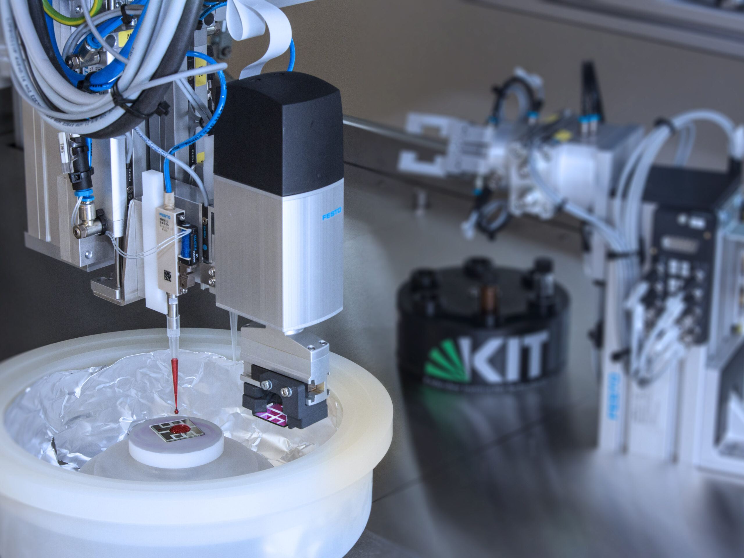
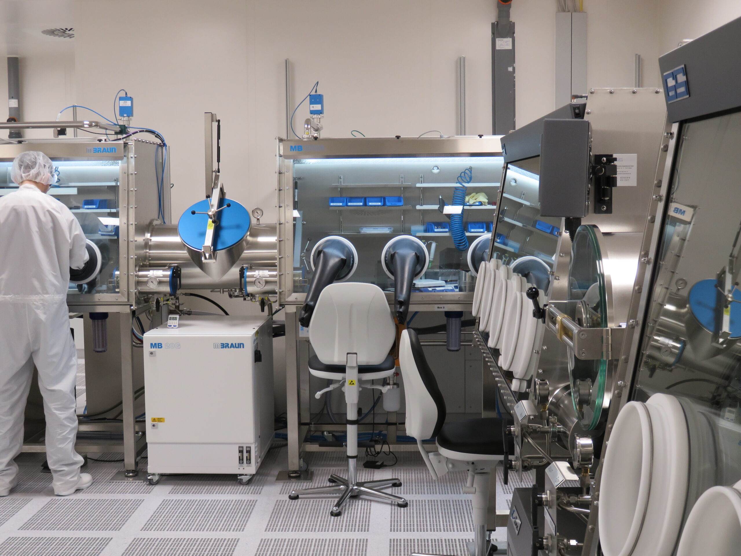
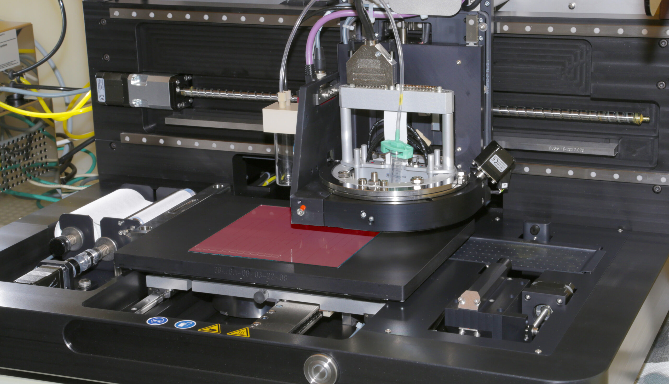
Purpose: The Organic PV Lab provides a comprehensive research environment for organic solar cell development—from molecular formulation to device testing. Its infrastructure includes a cluster of vacuum-based deposition systems, femtosecond laser ablation tools, and multiple coating techniques ranging from spin to slot-die, enabling complete multilayer device stacks. Furthermore, the lab integrates high-throughput automation workflows and advanced diagnostics for rapid material screening and combinatorial process optimization. These capabilities make the MZE Lab a versatile platform for both fundamental research and technology upscaling.
Unique Features
- Integration of inert and ambient processing across all key layer types
- Multi-chamber cluster tool for controlled evaporation of complex organic stacks
- High-precision fs laser ablation for device structuring at multiple wavelengths
- Fully equipped for OLED characterization alongside photovoltaics
- Extensive high-throughput automation for film deposition, characterization, and combinatorial material screening
- In-house capabilities for thermal processing up to 1500 °C
- Dedicated tools for long-term device stability assessment in accordance with ISOS and IEC standards
Processing Capabilities
Active Layers
- Spin and doctor blade coating (in inert and ambient environments)
- Film pulling (inert and ambient)
- Horizontal dip coating
- Spray coating, inkjet printing, slot-die coating
- Evaporation using cluster tools
Electrodes
- High vacuum evaporation system (metals)
- Cluster tool with 5 chambers (4 organic sources)
- Evaporator with 3 metal sources
Packaging & Miscellaneous
- CO₂ snow-jet for cleaning
- Sintering up to 1500 °C
- Encapsulation station
Transport Layers
- Deposition and integration of electron/hole transport layers
Patterning
- Femtosecond laser ablation with tunable wavelength (260 nm – 2.6 μm)
- Nanosecond laser system
Lab Automation & High-Throughput Screening
- Spin coating and quality assessment
- Combinatorial precursor solution mixing
- Photoluminescence (PL) and UV-Vis spectroscopy
- Sample handling, dynamic light scattering (DLS)
- Dispensing and storage of nanoparticle dispersions for high-throughput microfluidic ink preparation
Characterization Capabilities
Devices
- Solar simulator (xenon and LED; inert and ambient)
- External quantum efficiency (EQE) for single-junction and tandem devices (280 nm – 1.8 μm)
- Dark lock-in thermography (LiT)
- Local photocurrent mapping (LBIC)
- Electroluminescence (EL) including imaging
- Impedance spectroscopy and CELIV
- Space charge limited current (SCLC) measurements
- OLED characterization (integrating sphere, luminance, excited state dynamics)
Stability
- Lifetime measurement stations for organic solar cells and OLEDs
- Climate chamber with integrated solar simulator
- Measurements according to ISOS and IEC standards
Materials & Layers
- White light interferometry, confocal and digital optical microscopy
- Atomic force microscopy in inert (AFM, KPFM, c-AFM, pc-AFM, PFM)
- Photoelectron spectroscopy in air (PESA)
- UV-Vis spectroscopy
- Contact angle measurement
- Four-point probe (sheet resistance)
- ZETA potential, dynamic light scattering
- Time-resolved luminescence, photoluminescence quantum yield
- Profilometer
- Cryostat (10 K He)
Contact Person
Karlsruhe Institute of Technology (KIT)
Prof. Dr. Alexander Colsmann alexander.colsmann(at)kit.edu
Contact Person
Karlsruhe Institute of Technology (KIT)
Dr. Christian Sprau christian.sprau(at)kit.edu