Helmholtz Innovation Lab HySprint & KOALA
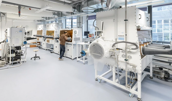
The combined HySprint and KOALA lab in Berlin serves as a key innovation hub for scalable deposition and advanced characterization of perovskite and tandem solar cells.

Overview
The combined HySprint and KOALA lab in Berlin serves as a key innovation hub for scalable deposition and advanced characterization of perovskite and tandem solar cells. By uniting HySprint’s expertise in inkjet and slot-die printing with KOALA’s advanced infrastructure for large-area device fabrication and industrial reliability testing, the lab enables a rapid transition from research to real-world application.
The lab supports both fundamental research and industry collaboration through high-throughput processes, in-situ diagnostics, and open-format workshops.
Detailed Description
Purpose:
HySprint & KOALA aims to drive the development and industrial scaling of next-generation solar technologies—especially perovskite-silicon tandem solar cells—by integrating lab-scale innovation with production-ready techniques. The lab promotes a smooth pathway from material discovery to commercial viability through a unique combination of processing, diagnostics, and long-term stability testing.
Focus Areas:
- Scalable processing for perovskite and perovskite/silicon tandem solar cells
- Integration of R&D with industry-grade testing and reliability analysis
- Development of highly reproducible, stable solar modules
- Hosting of demonstration workshops and industry collaborations
Unique Features
- Industrial-grade infrastructure for both inkjet printing (IJP) and slot-die coating (SDC), from lab to pilot scale
- Large-area processing up to 18 × 18 cm for perovskite and tandem solar cells
- Advanced inline and in-situ characterization using optical, electrical, and X-ray methods
- Laser processing in inert environments and packaging under controlled conditions
- Capability to test up to 1024 devices for long-term stability (MPP tracking, outdoor testing)
- Expertise in organizing workshops, open labs, and demos for academic and industrial partners
Processing Capabilities
Active Layers
- Spin coating
- Sheet-to-sheet (S2S) slot-die coating
- Inkjet printing (IJP)
- Blade coating (up to 18 × 18 cm)
- Large-area absorber evaporation (5-source system)
- Vacuum Thermal Deposition (VTD, in planning)
Electrodes
- Thermal evaporation
- High vacuum evaporation in cluster tools
- Atomic Layer Deposition (ALD)
- Inline sputtering tools
Transport Layers
- Spin coating
- Slot-die coating
- Uses same tools as electrode processing
Patterning
- Laser processing (under inert gas)
- Inkjet patterning
Packaging
- Off-line packaging setup
- Laminator / heat press using sealing compounds
Characterization Capabilities
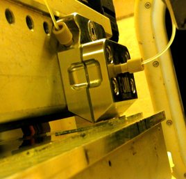
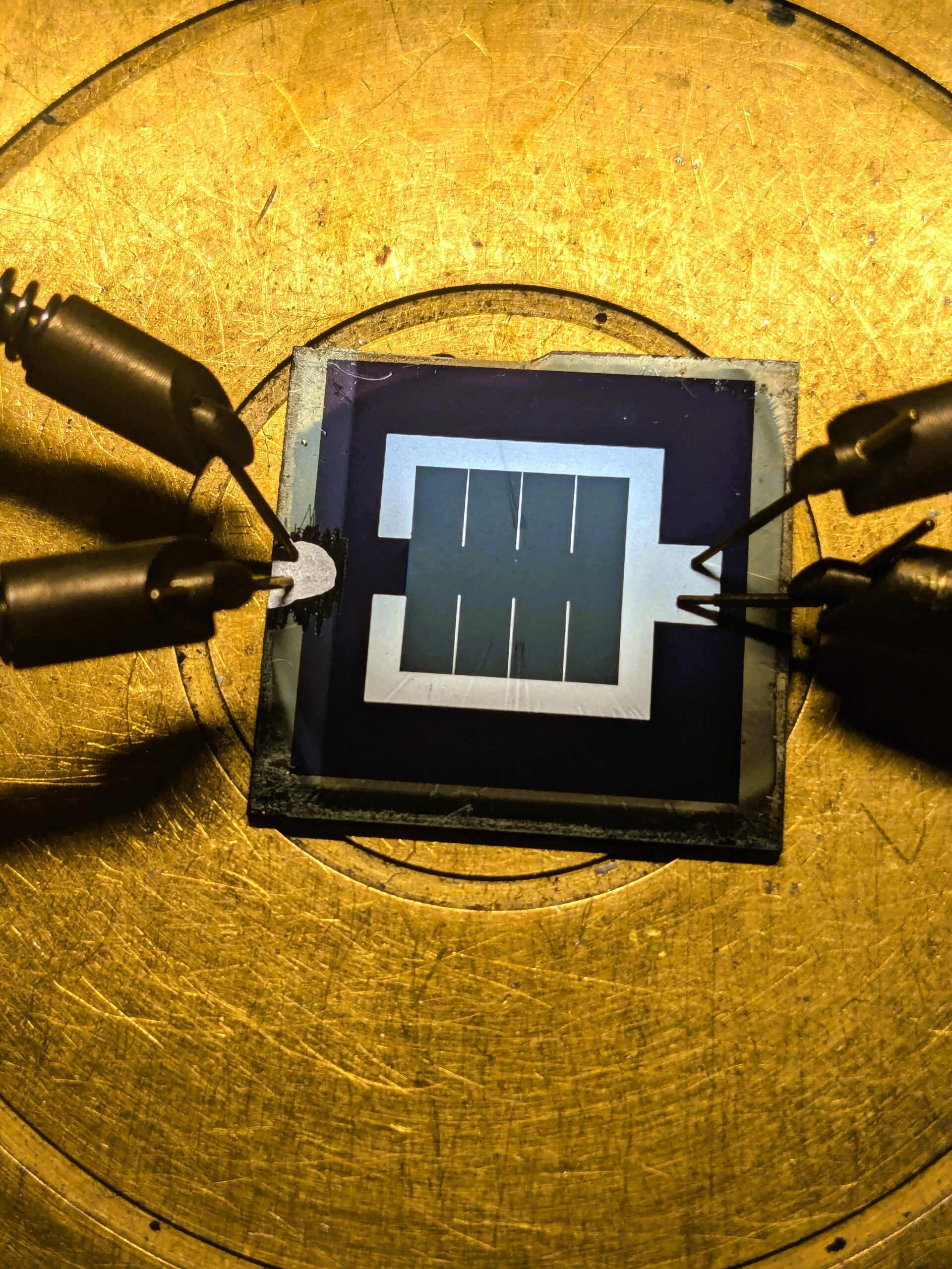
Devices
- Solar simulators (ambient & inert)
- External Quantum Efficiency (EQE) for single and tandem devices
- Dark lock-in thermography (DLiT)
- Light Beam Induced Current (LBIC) mapping
- Electroluminescence (EL) and thermography
- Band Alignment & Contact Extraction (BACE)
- Charge Extraction by Linearly Increasing Voltage (CELIV)
In-line / In-situ Methods
- Photoluminescence (PL)
- UV-Vis transmission and reflectance
- Fourier Transform Photocurrent EQE
- Grazing Incidence Wide-Angle X-ray Scattering (GIWAXS at BESSY II)
Materials & Layers
- Profilometry
- Atomic force microscopy (AFM)
- Scanning electron microscopy (SEM)
- UV-Vis spectroscopy
- Time-resolved PL
- PL and EL mapping
- X-ray diffraction (XRD) and fluorescence (XRF)
- Sheet resistance (four-point probe)
- PL imaging (in setup phase)
Stability
- Stability testing for up to 1024 devices
- MPP tracking setups
- Lifetime test stations
- Outdoor test stand (up to 48 cells)
- Climatic chamber
- Tandem cell testing under inert conditions (24 cells)
Further information
Contact Person
Prof. Dr. Eva Unger
eva.unger(at)helmholtz-berlin.de
Contact Person
Dr. Jona Kurpiers
jona.kurpiers(at)helmholtz-berlin.de