Perovskite lab at KIT
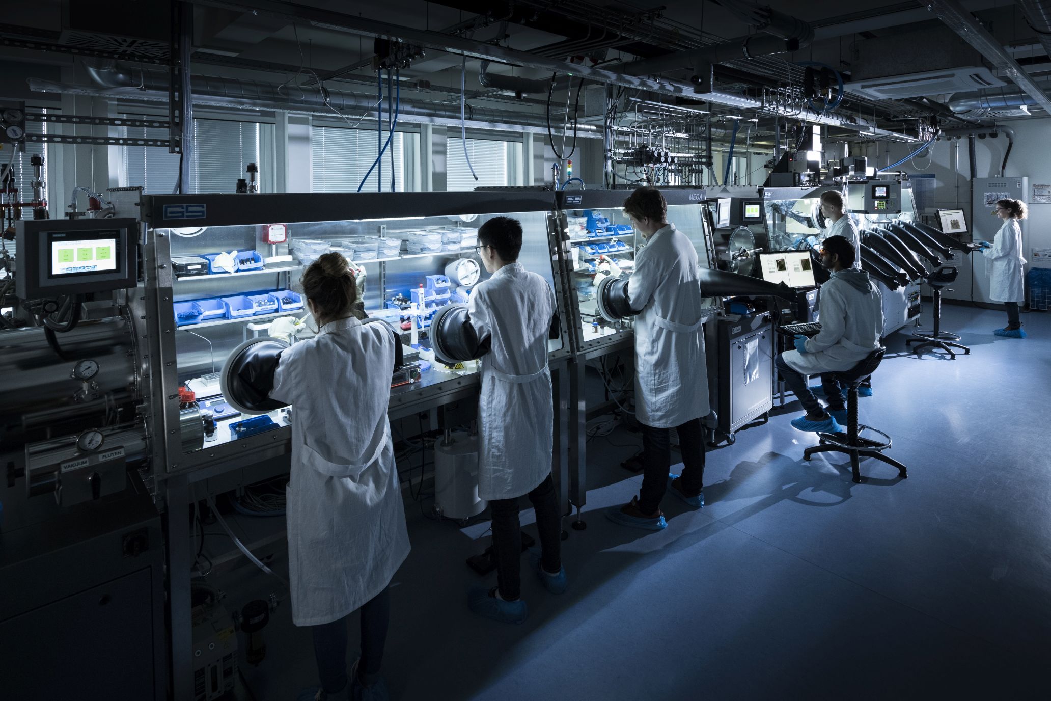
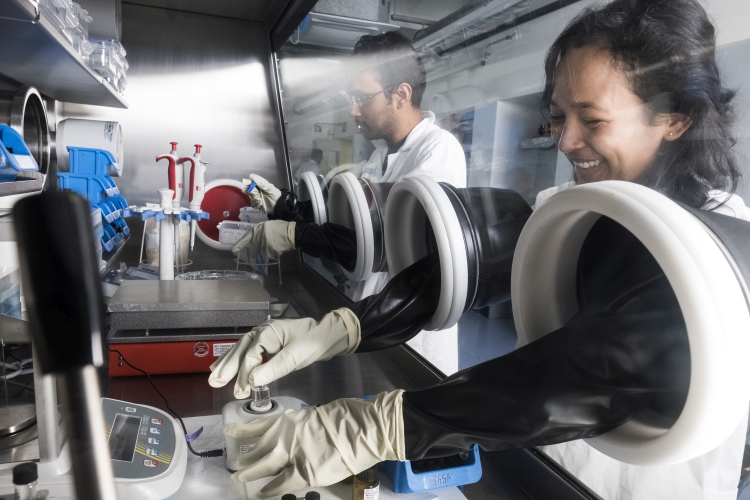
The Perovskite lab at KIT focuses on high-efficiency device concepts for perovskite-based photovoltaics.
Combining advanced thin-film deposition techniques with comprehensive characterization capabilities, the lab supports the development of tandem, semi-transparent, and scalable solar cell architectures.


Overview
Led by Prof. Ulrich Pätzold and Prof. Ulrich Lemmer, the Perovskite Lab at KIT is equipped for cutting-edge research on perovskite and hybrid solar cells. The lab combines precision coating and laser structuring with optical and electrical evaluation, targeting novel materials and device designs. A strong focus lies in developing scalable tandem solar cell architectures, including perovskite/silicon, perovskite/CIGS, and triple-junction concepts.
Detailed Description
Purpose: The lab infrastructure enables the fabrication of complex multilayer stacks via spin coating, blade coating, slot-die, and inkjet printing on areas up to 30×40 cm. Drying processes are supported by Slot Jet, IR, and 2D systems. Electrode and transport layers are applied using various evaporation tools, including ebeam and process gas sputtering. Laser-based patterning in inert atmosphere is used for precise structuring. Characterization spans from photoluminescence and Raman spectroscopy to time-resolved and in-situ optical methods, as well as white light interferometry and transient absorption. Stability testing includes MPP tracking in controlled atmospheres and outdoor operation of up to 24 cells.
Unique Features
- Large-area processing up to 30 × 40 cm using spin, slot-die, blade, and inkjet coating
- Multi-source evaporation systems and ebeam deposition under inert or reactive conditions
- Integrated Slot Jet, IR, and 2D drying for tailored layer formation
- Optical and spectroscopic toolset including Raman, PLQY, and transient absorption
- Stability testing with MPP tracking in inert conditions and outdoor setups (up to 24 cells)
- Laser patterning in inert atmosphere for high-precision device definition
- Advanced tandem architectures: perovskite/Si, perovskite/CIGS, and perovskite/perovskite
- Focus on translucent devices and upscaling strategies
Processing Capabilities
Active Layers
- Spin coating, spin-bot, slot-die (up to 30×40 cm)
- Blade coating, inkjet printing (up to 30×40 cm)
- Two evaporation systems (5 sources and 6 sources)
- Combinatorial materials/solution preparation
- Drying systems: Slot Jet, IR, 2D drying system
Electrodes
- Several evaporators, ebeam evaporation with process gas
- Sputtering system
Transport Layers
- ebeam evaporation
Patterning
- Laser structuring in inert atmosphere
Lab Automation & High-Throughput Screening
- Spin coating and quality assessment
- Combinatorial precursor solution mixing
- Photoluminescence (PL) and UV-Vis spectroscopy
- Sample handling, dynamic light scattering (DLS)
- Dispensing and storage of nanoparticle dispersions for high-throughput microfluidic ink preparation
Characterization Capabilities
Devices
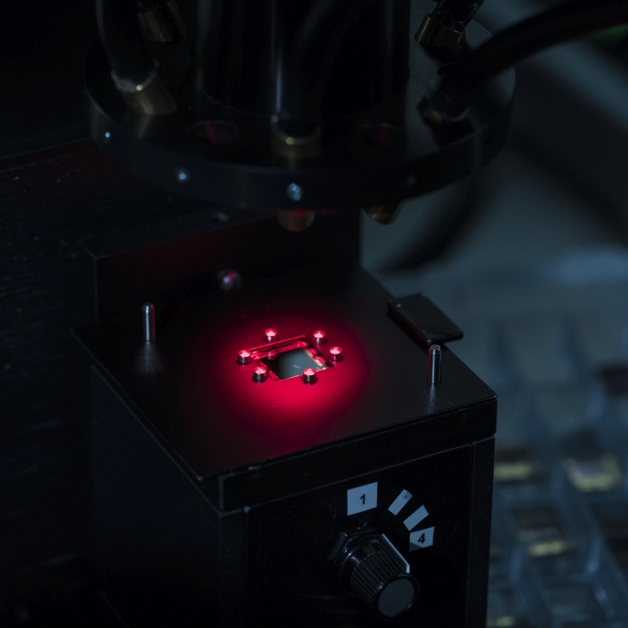
- Solar simulator (inert, LED, Xenon)
- External quantum efficiency (EQE) under inert conditions
- LBIC, photoluminescence (PL) and electroluminescence (EL) imaging
- CELIV measurements
Stability
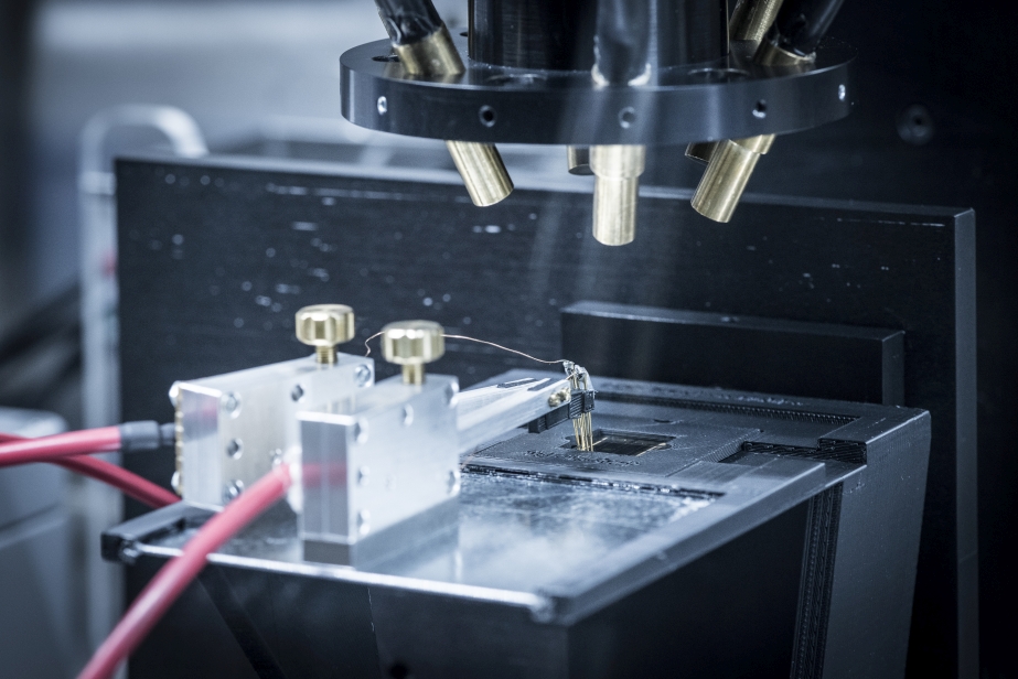
- Up to 16 cells in inert atmosphere holders with MPP tracking
- Controlled temperature setups, up to 24 cells tested outdoors
Materials & Layers
- Raman spectroscopy, time-resolved PL
- In-situ reflection spectroscopy
- PL and EL mapping, white light interferometry, PLQY
- Transient absorption spectroscopy
Further information
Contact Person
Prof. Dr. Ulrich Paetzold
ulrich.paetzold(at)kit.edu
Contact Person
Dr. Paul Faßl
paul.fassl(at)kit.edu